Nanoparticles
Abstract
Nanoparticles were being used even before the 4th century AD, but artists were unaware of what cause these unique, beautiful optical effects. The most prevalent use of nanoparticles has always been for their optical properties. Only in recent times have nanoparticles come under the scrutiny of researchers, and they have revealed several more uses, which are elaborated ahead.
With the advent of methods to observe and create particles of these sizes, we can explain the structure and properties of nanoparticles, and with that knowledge, create particles of desired size, to fit its specific need.
Quantum dots has become a hotly discussed topic, with its discovered use in monitors and screens.
Introduction
Nanotechnology is the science that deals with matter at the scale of 1 billionth of a meter (i.e., 10− 9 m = 1 nm), and is also the study of manipulating matter at the atomic and molecular scale
A nanoparticle is the most fundamental component in the fabrication of a nanostructure, and is far smaller than the world of everyday objects that are described by Newton’ s laws of motion, but bigger than an atom or a simple molecule that are governed by quantum mechanics
The size of a nanoparticle spans the range between 1 and 100 nm. Metallic nanoparticles have different physical and chemical properties from bulk metals (e.g., lower melting points, higher specific surface areas, specific optical properties, mechanical strengths, and specific magnetizations), properties that might prove attractive in various industrial applications
Nanoparticles can be amorphous or crystalline. Being small in size, crystalline nanoparticles can be of single domain. Nanoparticles of metals, chalcogenides, nitrides, and oxides are often single crystalline. Crystalline nanoparticles are referred to as nanocrystals.
Nanoclusters consist of a small number of atoms, at most in the tens. These nanoclusters can be composed either of a single or of multiple elements, and typically measure less than 2mm. Such nanoclusters exhibit attractive electronic, optical, and chemical properties compared to their larger counterparts. Materials can be categorized into three different regimes, namely bulk, nanoparticles/ nanostructures and atomic clusters. Bulk metals are electrical conductors and good optical reflectors, while metal nanoparticles display intense colours due to surface plasmon resonance. When the size of metal nanoclusters is further reduced, to 1nm or less, in other words to just a few atoms, the band structure becomes discontinuous and breaks down into discrete energy levels, somewhat similar to the energy levels of molecules. Therefore, a nanocluster behaves like a molecule and does not exhibit plasmonic behaviour; nanoclusters are known as the bridging link between atoms and nanoparticles.
1. Nanoparticles and Nanocrystals
In general, the size of a nanoparticle spans the range between 1 and 100 nm. Metallic nanoparticles have different physical and chemical properties from bulk metals (e.g., lower melting points, higher specific surface areas, specific optical properties, mechanical strengths, and specific magnetizations), properties that might prove attractive in various industrial applications.
1.1 Properties of Nanoparticles/Nanocrystals
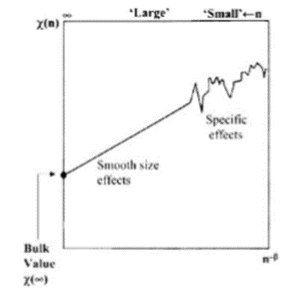
The diameters of nanoparticles can vary anywhere between one and a few hundreds of nanometres. Small nanoparticles with diameters of a few nanometres are comparable to molecules. Accordingly, the electronic and atomic structures of such small nanoparticles have unusual features, markedly different from those of the bulk materials. Large nanoparticles (>20–50nm), on the other hand, would have properties similar to those of the bulk. The change in a material property as a function of size is shown schematically in Fig.2.1.1. At small sizes, the properties vary irregularly and are specific to each size. At larger sizes, dependence on size is smooth and scaling laws can be derived to describe the variation in this regime. The size-dependent properties of nanoparticles include electronic, optical, magnetic, and chemical characteristic
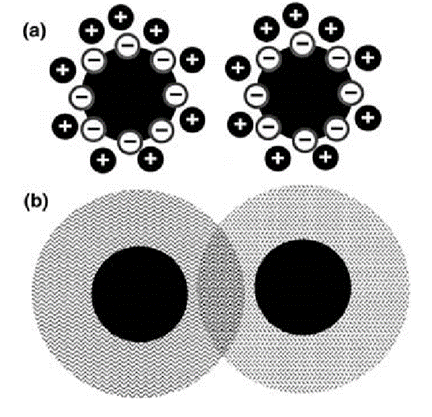
Nanocrystals of materials are generally obtainable as sols. Sols containing nanocrystals behave like the classical colloids. For example, the stability of a dispersion depends on the ionic strength of the medium. Nanocrystalline sols possess exceptional optical clarity. A key factor that lends stability to nanocrystal sols is the presence of a ligand shell, a layer of molecular species adsorbed on the surface of the particles. Without the ligand shell, the particles tend to aggregate to form bulk species that flocculate or settle down in the medium. Depending on the dispersion medium, the ligands lend stability to particles in two different ways. Thus, in an aqueous medium, coulomb interactions between charged ligand species provide a repulsive force to counter the attractive van der Waals force between the tiny grains, by forming an electrical double layer. In an organic medium, the loss of conformational freedom of the ligands and the apparent increase in solute concentration provide the necessary repulsive force. This is illustrated schematically in Fig.2.1.2. Nanocrystals dispersed in liquids are either charge-stabilized or sterically stabilized. Nanoparticles devoid of ligands are generally studied in vacuum. Such particles deposited on a substrate are readily examined by photoelectron spectroscopy and other techniques. Beams of uniformly sized clusters traversing a vacuum chamber (cluster beams) with some fixed velocity provide opportunities for studies of the intrinsic physical properties of nanoparticulate matter
1.2 History of Nanoparticles
The optical characteristics of nanoparticles have been used from time immemorial in sculptures and paintings even before the 4th century AD. The most famous example is the Lycurgus cup (fourth century AD) illustrated in Figure 2.2.1

It is the presence of these nanocrystals that gives the Lycurgus Cup its special colour display.
Analysis of the glass revealed that it contains a very small quantity of tiny (∼70 nm) metal crystals of Ag and Au in an approximate molar ratio of 14: 1, which give it these unusual optical properties. It is the presence of these nanocrystals that gives the Lycurgus Cup its special colour display.
Soluble gold appeared around the fifth or fourth century B.C. in Egypt and China. Until the Middle Ages, the reputation of soluble gold was based mostly on its fabulous curative powers of various diseases, for example, heart and venereal diseases, dysentery, epilepsy, and tumours.
A colorant in glasses, that is, the “Purple of Cassius”, was a colloid resulting from the presence of gold particles and tin dioxide and was highly popular in the seventeenth century
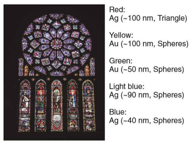
Nanotechnology is easily evident in various old churches. A well-known application of early nanotechnology is the ruby red colour that was used for stained glass windows during the Middle Ages.
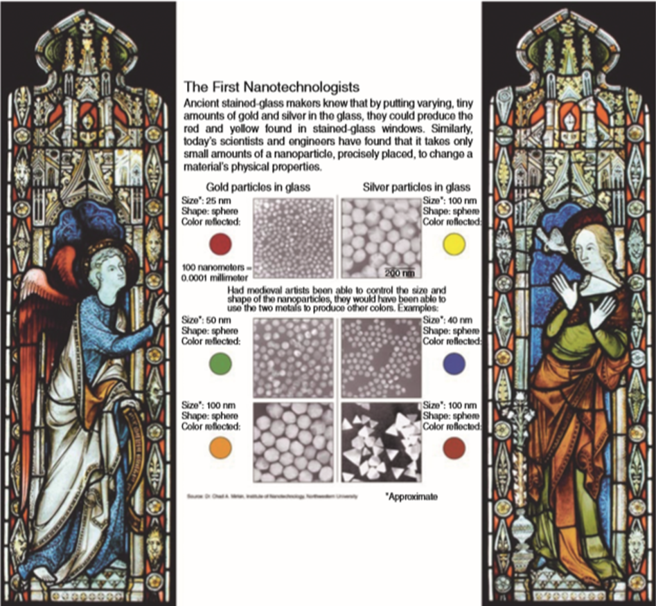
Beautiful examples of these applications can be found in glass windows of many Gothic European cathedrals as seen in Fig .1.2.3.
Nanoparticles of carbon black (tire soot) have been used in the fabrication of rubber tires of automobiles from the beginning of the twentieth century
Despite the early advances, studies of nanoscale particles did not gather momentum in later years. Thus, for most part of the 20th century, colloid science was the domain of a few specialized groups and did not receive sufficient importance
1.3 Synthesis of Nanoparticles
Before the 17th century, the ability to synthesize nanoparticles preceded the understanding of nanoscale phenomenon. In recent times, owing to the need for manipulating of dimensions of nanoparticles for different uses, there has been an emergence of many methods to synthesize Nanoparticles, summarized in Figure 2.3.1
Two approaches have been known in the preparation of ultrafine particles from ancient times. The first is the breakdown (top-down) method by which an external force is applied to a solid that leads to its break-up into smaller particles. The second is the build-up (bottom-up) method that produces nanoparticles starting from atoms of gas or liquids based on atomic transformations or molecular condensations
he top-down method is the method of breaking up a solid substance; it can be sub-divided into dry and wet grinding. In the dry grinding method, the solid substance is ground as a result of a shock, a compression, or by friction, using such popular methods as a jet mill, a hammer mill, a shearing mill, a roller mill, a shock shearing mill, a ball mill, and a tumbling mill. Since condensation of small particles also takes place simultaneously with pulverization, it is difficult to obtain particle sizes of less than 3 μ m by grain refining. On the other hand, wet grinding of a solid substrate is carried out using a tumbling ball mill, or a vibratory ball mill, a planetary ball mill, a centrifugal fluid mill, an agitating beads mill, a flow conduit beads mill, an annular gap beads mill, or a wet jet mill. Compared with the dry method, the wet process is suitable for preventing the condensation of the nanoparticles so formed, and thus it is possible to obtain highly dispersed nanoparticles
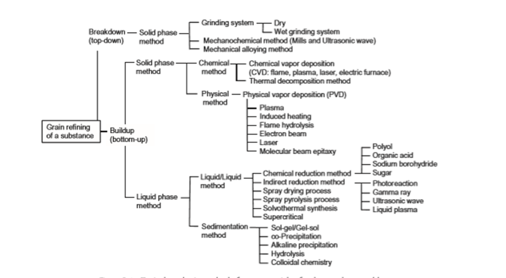
The bottom-up approach is roughly divided into gaseous phase methods and liquid phase methods. For the former, the chemical vapor deposition method (CVD) involves a chemical reaction, whereas the physical vapor deposition method (PVD) uses cooling of the evaporated material. Although the gaseous phase methods minimize the occurrence of organic impurities in the particles compared to the liquid phase methods, they necessitate the use of complicated vacuum equipment whose disadvantages are the high costs involved and low productivity. The CVD procedure can produce ultrafine particles of less than 1 μm by the chemical reaction occurring in the gaseous phase. The manufacture of nanoparticles of 10 to 100 nm is possible by careful control of the reaction. Performing the high temperature chemical reaction in the CVD method requires heat sources such as a chemical flame, a plasma process, a laser, or an electric furnace. In the PVD method, the solid material or liquid material is evaporated and the resulting vapor is then cooled rapidly, yielding the desired nanoparticles
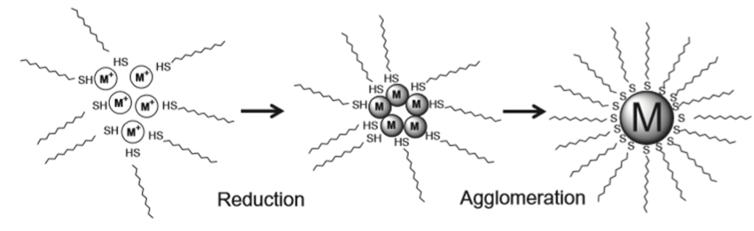
For many years, liquid phase methods have been the major preparation methods of nanoparticles; they can be sub-divided into liquid/liquid methods, and sedimentation methods. Chemical reduction of metal ions is a typical example of a liquid/ liquid method, whose principal advantage is the facile fabrication of particles of various shapes, such as nanorods, nanowires, nanoprisms, nanoplates, and hollow nanoparticles. With the chemical reduction method, it is possible to fi ne-tune the form (shape) and size of the nanoparticles by changing the reducing agent, the dispersing agent, the reaction time and the temperature.
Besides the chemical reduction method which adds a reducing agent (direct reduction method), other reduction methods are known, such as photoreduction using gamma rays, ultrasonic waves, and liquid plasma which can be used to prepare nanoparticles. These methods that do not use a chemical reducing substance have the attractive feature that no extraneous impurities are added to the nanoparticles. Other than these methods, spray drying, spray pyrolysis, solvothermal synthesis, and the supercritical method are also known. The general technique in the sedimentation method is a sol–gel process, which has been used extensively for the fabrication of metal oxide nanoparticles. This procedure transforms a solution of a metal alkoxide into a sol by hydrolysis, followed by polycondensation to a gel.
The wet process (liquid phase method) guarantees a high dispersivity of nanoparticles compared to the dry method. However, if the resulting nanoparticles are dried, aggregation of the particles soon follows. In this case, re-dispersion can be carried out according to the process used in the solid phase method. There are some features to consider that are common to all the methods. That is, the synthesis of nanoparticles requires the use of a device or process that fulfills the following conditions:
• control of particle size, size distribution, shape, crystal structure and composition distribution
• improvement of the purity of nanoparticles (lower impurities)
• control of aggregation
• stabilization of physical properties, structures and reactants
• higher reproducibility
• higher mass production, scale-up and lower costs
1.4 Structure of Nanoparticles
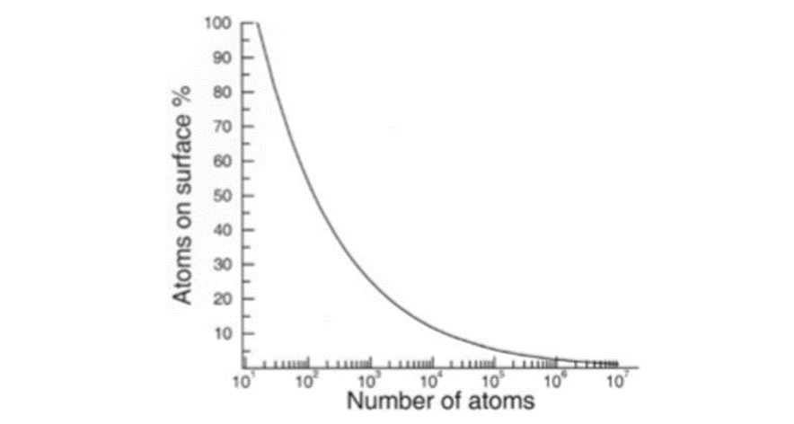
The dimensions of nanocrystals are so close to atomic dimensions that an unusually high fraction of the total atoms would be present on their surfaces. For example, a particle consisting of 13 atoms, would have 12 atoms on the surface, regardless of the packing scheme followed. We see that the fraction of surface atoms becomes less than 1% only when the total number of atoms is of the order of 107, which for a typical metal would correspond to a particle diameter of 150nm.
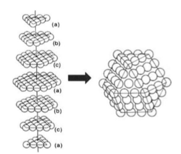
Nanoparticles are generally assumed to be spherical. However, an interesting interplay exists between the morphology and the packing arrangement, especially in small nanocrystals. If one were to assume that the nanocrystals strictly follow the bulk crystalline order, the most stable structure is arrived at by constraining the number of surface atoms. It is reasonable to assume that the overall polyhedral shape has some of the symmetry elements of the constituent lattice. Polyhedra such as the tetrahedron, the octahedron and the cuboctahedron can be constructed following the packing scheme of a fcc lattice . Figure 2.4.2 shows how a cuboctahedral cluster of 146 constituent atoms follows from a fcc type abcabc layer stacking. In contrast to the above, small clusters frequently adopt non-close packed icosahedral or dodecahedral shapes.
Several theoretical investigations have sought to explain the unusual stability of icosahedral clusters. They, based on potential energy calculations, showed that the binding energy per atom is lower than that in a corresponding octahedron containing the same number of atoms. Molecular dynamics simulations have shown that Al clusters with nuclearities upto 147 atoms exhibit distorted icosahedral structures while Al147 has a cuboctahedral shape
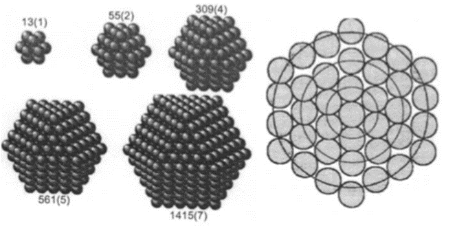
The properties of nanocrystals are also influenced by the formation of geometric shells which occur at definite nuclearities. Such nuclearities, called magic nuclearities endow a special stability to nanocrystals as can be demonstrated on the basis of purely geometric arguments. A new shell of a particle emerges when the coordination sphere of an inner central atom or shell (forming the previous shell) is completely satisfied. The number of atoms or spheres required to complete successive coordination shells is a problem that mathematicians, starting with have grappled with for a long time
Determination of the structures of nanocrystals should ideally follow from X-ray diffraction, but small particles do not diffract well owing to their limited size. The peaks in the diffraction pattern are less intense and are broad. Structural studies are therefore based on high resolution transmission electron microscopy (HRTEM), extended X-ray absorption fine structure (EXAFS), scanning tunneling microscopy (STM) and atomic force microscopy (AFM). X-ray diffraction patterns provide estimates of the diameters (D) of nanocrystals from the width of the diffraction profiles
1.5 Surface Plasmon Resonance and Colouring
The physical phenomenon of surface plasmon resonance (SPR) was reported long ago by Wood who could detect sub-monomolecular coverage [3]. Not only did Wood discover the plasmon resonance phenomenon, but also found that it changed with the composition of the liquid in touch with the metal surface. Although he speculated on how the light, grating and the metal interacted with each other, a clear rationalization of the phenomenon was not provided. He observed a pattern of “anomalous” dark and light bands in the refracted light when he shone polarized light on a mirror with a diffraction grating on its surface. The first theoretical treatment of these anomalies was put forward by Rayleigh in 1907 [4]. Rayleigh’ s “dynamical theory of the grating” was based on an expansion of the scattered electromagnetic field in terms of outgoing waves only. With this assumption, he found that the scattered field was singular at wavelengths for which one of the spectral orders emerged from the grating at the grazing angle. He then observed that these wavelengths, which have come to be called the Rayleigh wavelengths,
λR, correspond to the Wood anomalies, but a complete explanation of the phenomenon was not possible until 1968 when Otto [5], and in the same year Kretschmann and Raether [6], reported the excitation of the surface plasmon band.
Surface plasmon resonance has also been similarly researched in solid state physics in recent years in application studies, especially in such applied research as biosensing, solar cells, and super high-density recording.
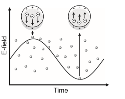
In solid state physics, the plasmon represents the collective oscillation of a free charge in a metal, and may be considered as a kind of plasma wave. The positive electrical charge in the metal is fixed and the free electron is free to move around it. An applied external electric field, as from a light source, causes the free electrons at the surface of the metal to vibrate collectively, giving rise to surface plasmons. Since electrons are also particles with an electric charge, when they vibrate they also generate an electric field, and when the electric field from the vibration of free electrons and the applied external electric field (e.g., electromagnetic waves) resonate the resulting phenomenon is referred to as a surface plasmon resonance that takes place at the surface of the metal. However, if light irradiates a solution that contains dispersed metal nanoparticles smaller than the wavelength of light, then depending on the electric field of light, the deviation produces a free electron at the surface of the metal. As a result, the weak or thick portions of the electric field appear on the nanoparticle surface (Figure 1.5.1) and can be considered as a kind of polarization. Such localized plasmon resonance is called localized surface plasmon resonance (LSPR).
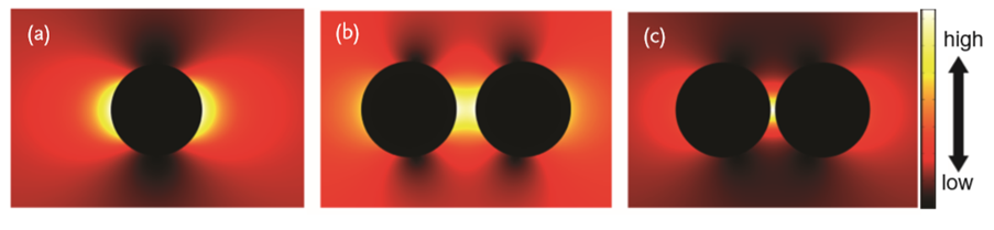
The LSPR is typically concentrated in a very narrow region on the surface of a nanoparticle. The electric field distribution on the nanoparticle surface caused by LSPR can be visualized using an electromagnetic field analysis software with a finite element method. The LSPR distribution on the surface of a 20-nm (diameter) Au nanoparticle is shown in Figure 1.5.2 a When visible light at 520 nm, which corresponds to the maximum position of the LSPR band in the Au nanoparticle, is used to irradiate the nanoparticle, the electric field generated is concentrated on the right and left side of the Au nanoparticle, perpendicular to the incident light direction. On the other hand, the electric field generated in two adjacent Au nanoparticles is concentrated within the gap between the two particles. Figure 1.5.2 b illustrates two particles with a 4-nm gap, while Figure 1.5.2 c displays two particles separated by a gap of 1 nm. As the gap becomes narrower and narrower, the density of the generated electric field gets bigger and bigger.
The wavelength corresponding to the LSPR depends on the kind of metal, the shape of the metal nanoparticle, and the extent of aggregation of the metallic nanoparticles. Moreover, the surface plasma vibration also changes with the dielectric constant and the quality of the carrier fluid. The plasma oscillations in the metal occur mainly in the ultraviolet (UV) region. However, in the case of Au, Ag, and Cu, the plasma shifts nearer to the visible light domain with the band due to electrons in the s atomic orbitals. For example, the wavelength of the surface plasmon resonance band maximum of a spherical Au nanoparticle is 520–550 nm. If a colloidal Au nanoparticle solution is now irradiated with visible light at these wavelengths (520–550 nm), the visible light corresponding to the green colour is absorbed and the particles now display a red purple colour, which is the complementary colour to green. In a colloidal Ag nanoparticle solution which has a plasmon resonance band maximum near 400 nm, the blue colour of the visible light is absorbed and the Ag particles now take on a yellow colour, the complementary colour to blue.
1.6 Control of Size and Shape
1.6.1 Size Control of Nanoparticles
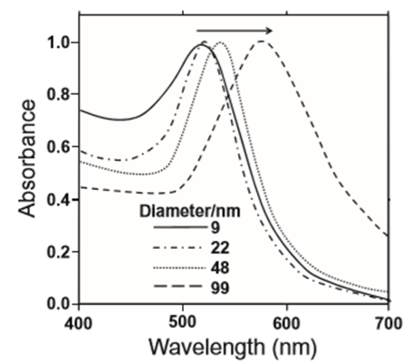
The physical and chemical properties of nanomaterials depend not only on their composition but also on the particle size and shape. Accordingly, a high-quality synthesis protocol must first of all provide control over particle size and shape. For example, if the diameter of an Au nanosphere is made to increase, the surface plasmon resonance will be gradually shifted from 530 nm to the longer wavelength side (Figure 2.6.1.1). Thus, if nanoparticles differ in size, their optical characteristics will also change significantly.
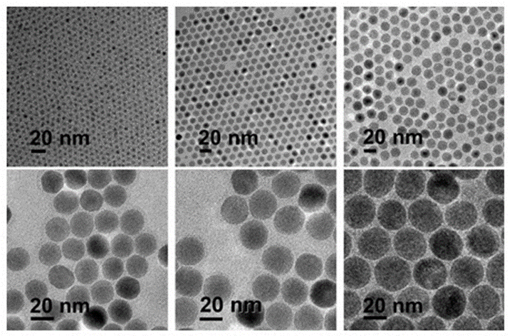
In optical applications of nanoparticles, simplification of the size distribution of the particles becomes a very important factor. Therefore, it is important to fabricate nanoparticles with a single target size in mind. Generally, in order to prepare monodispersed nanoparticles, it is imperative that the nanoparticles grow very slowly after the rapid generation of the seed particles
If the size of the nanoparticles decreases (i.e., increase in specific surface area), then the increase in the surface energy of such nanoparticles will facilitate their aggregation. Consequently, after their growth to the desired optimal size, it will be necessary to stabilize the particulate surface by addition of a dispersing agent.
As shown in Figure 2.6.1.2, if 1-dodecanethiol is used as the dispersing agent in Au nanoparticle synthesis the 1-dodecanethiol molecule can form a monomolecular layer on the Au nanoparticle surface, and firmly stabilize the dispersed Au nanoparticles.
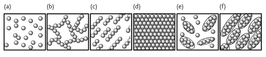
It is important to realize that the physical properties of a nanoparticle can change with the aggregation ratio, even though the colloidal solution may contain nanoparticles of identical size. The images and the characteristics of the state of aggregation of nanoparticles are depicted in Figure 2.6.1.3. In the dispersed random structure shown in Figure 2.6.1.3 a, the dynamical physical properties and the optical properties are significant. On the other hand, the electronic properties are displayed by the fractal structure shown in Figure 2.6.1.3 b, and ion and electronic transport properties appear in the structure orientation of Figure 2.6.1.3 c. The optical properties appear in the close-packed structure of the nanoparticles (Figure 2.6.1.3 d), whereas the discrete structures or otherwise orderly structures of Figure 2.6.1.3 e and f display dynamical physical properties, magnetism, optical, and electronic properties.
Methods to separate out particles of a given target size from a colloidal solution which contains nanoparticles of various sizes are known. They are (i) separation by precipitation, (ii) centrifugal separation, (iii) gel filtration column, and (iv) gel electrophoresis. As a feature of each screening method, the precipitation separation is suitable for a large distribution of colloid nanoparticles in the solution. The centrifugal separation and the gel fi ltration column are well suited for solutions of colloidal nanoparticles with a narrow size distribution. Gel electrophoresis is a suitable method to separate nanoparticles taking advantage of the difference in charge density of the particles, and is suitable for separating particles with a small cluster size. In fact, a combination of these various methods might prove advantageous. However, a problem with sorting the various sized nanoparticles using these methods is that only a fraction of the nanoparticles of a given size may be collected, and then only in small quantities. The digestive ripening method and high temperature melting technique have been proposed to resolve this problem
1.6.2 Shape Control of Nanoparticles
The shape of nanoparticles is an important factor that determines the nature of the surface plasmon resonance band just as the size of the nanoparticles did. Absorption spectra in the visible spectral region of various Au rodshaped nanoparticles (i.e., nanorods) with changes in the aspect ratio (length of long side and short side) are shown in Figure 2.6.2.1. The diameters of the Au nanorods espousing a pillar form and used in this experiment ranged from 5 to 20 nm and the lengths from 20 to 150 nm.
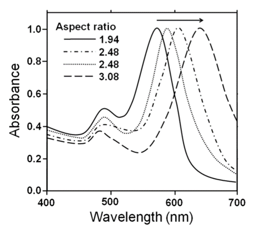
It is worth noting that the change in the ratio of a nanorod is related to the size ratio of a crystal face. An increase in the size ratio (aspect ratio) shifts the maximal absorption band to longer wavelengths. Therefore, the physical composition of the nanorods can easily change their spectroscopic features, such that various studies have been required to understand these characteristics.
In the initial stage, the nanosize porous alumina electrode is produced and the metal is then electrochemically deposited sequentially in the fi ne pores, which provide a firm mould; the diameter of the short axis of the Au nanorod which grows inside the fi ne pores is regulated by the size of the pores. Subsequently, the alumina mould is dissolved and removed; the so-formed Au nanorods are then taken out of the template. An interesting feature of the above method is the fabrication of nanorods of multiple layers of different metals such as Au–Ag–Au. Therefore, a nanoparticle with various features can be synthesized. As for the plural layer-type nanorod, applied research can lead to a nanosize system that might be considered a nanosized bar code
1.7 Application of Nanoparticles
1.7.1 Application of Metallic Nanoparticles
The various characteristics of different nanoparticles relative to bulk metals are summarized below.
Optical function: The surface absorption plasmon of Au and Ag can express various colours by changing the size of the particle, the form or shape of the particle, and the rate of condensation. A new paint that has the durability of an inorganic pigment and the vivid colour of an organic substrate can be made. Nanoparticles smaller than the wavelength of light can be used to make high penetration conductivity materials (there is little absorption, dispersion, and reflection).
One of the most interesting aspects of metal nanoparticles is that their optical properties depend strongly upon the particle size and shape. Bulk Au looks yellowish in reflected light, but thin Au films look blue in transmission. This characteristic blue colour steadily changes to orange, through several tones of purple and red, as the particle size is reduced down to ∼3 nm. The nanoparticles attracted attention as colour materials and the possibility of their use has been examined in various fields. Figure 2.7.1.1 illustrates the photograph of a car to which was applied a “clear coloured coating” containing gold nanoparticles on a base coating containing red pearl mica. Spraying with the clear coloured coating containing the nanoparticles increased the depth of the red background even more, and since the car is in the shade there is almost no diffuse reflection. The red colour becomes a feature of paints containing nanoparticles. Paints that contain nanoparticles cannot be removed as easily as can classical paint. However, because of high costs, paints with nanoparticles are used only in limited applications. Metal nanoparticles have also been used in enamel colour paints in pottery. Conventional enamel colour has used paints with mixed transition metals in the pulverization (glass frit) of glass. If, instead of transition metal paints, Au nanoparticles were used, then high quality red paint could be made with high transparency. Research into iron oxide nanoparticles in paints has also been carried out.

Catalyst function: Reaction efficiencies can be enhanced since the specific surface area of such nanoparticles is large compared with existing particles; to the extent that the surface terrace is regular at the atomic level, a hyperactive catalyst with high selectivity can be made: for example, Au nanoparticles.
Ni, Pd, Ag, and Pt have been used as typical metal catalysts in chemical reactions. However, the dissociative adsorption of hydrogen or oxygen molecules cannot be carried out on an Au smooth surface and at a temperature of less than 200 °C. Therefore, such a gold material is inactive as a catalyst in hydrogenation and oxidation reactions. However, when Au nanoparticles are used, they work effectively as catalysts.
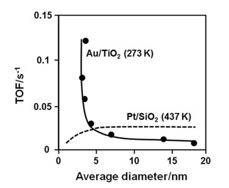
The ratio of the corner to the edge of an Au nanoparticle of several nanometers in size becomes large compared with Au particles of larger size. Thus, both the adsorption and the catalytic characteristics of the Au surface increase. In an icosahedron consisting of 2054 Au atoms, the percentage of Au atoms exposed on the surface is 15% in Au nanoparticles of 4.9 nm size (external diameters), whereas the surface exposure of an Au atom reaches 52% in 2.7 nm sized nanoparticles (309 Au atoms). If the number of Au atoms in a nanoparticle was to become even smaller, the number of atoms that constitutes the whole, as well as the electrons, will become limited since the electronic structure of the nanoparticle would then become discontinuous. This state takes on a cluster structure and a quantum size effect shows up in the physical properties. Generally, metals that form clusters of such a small size tend to be unstable to the atmosphere. However, Au clusters are stable and so Au can be used as a catalyst. The catalytic action is rapid as the size of the Au nanoparticle is small in catalyzed oxidation reactions. For example, in order to oxidize CO with a Pt catalyst, a temperature of not less than 100 °C is needed. However, with an Au nanoparticle as the catalyst, reaction can occur even at temperatures below 0 °C (see Figure 2.7.1.2).
Thermal function: When the particle diameter is small (less than 10 nm), the melting point is also lower than a bulk metal. Electronic wiring can be made with nanoparticles that have a low boiling point, for example, a polymer.
Electrical function: Since superconductivity transition temperature rises so that particle diameter is small (less than 1 nm), it can be used to make high temperature superconductivity material.
Medical function:
Polymer coated iron oxide nanoparticles (Shown in Fig 2.7.1.4) to break up clusters of bacteria, possibly allowing more effective treatment of chronic bacterial infections.
Mechanical function: Since the mechanical characteristics improve, mechanical strength can be sharply raised by mixing the nanoparticles with metals or ceramics.
Magnetic function: The attractive force of a magnetic metal increases on reduction of the particle diameter, such that soft-magnetic materials can be made in the form of an alloy of nanoparticles. Moreover, a permanent magnet can be made if the nanoparticles are smaller than the magnetic domain made to magnetize.
1.7.2 Nanotubes
A nanotube is a nanometre-scale tube-like structure. A nanotube is a kind of nanoparticle. The first nanotubes to be discovered were carbon nanotubes [16]
1.7.2.1 Carbon Nanotubes
Carbon nanotubes (CNTs) are allotropes of carbon with a cylindrical nanostructure. Owing to the material's exceptional strength and stiffness, nanotubes have been constructed with length-to-diameter ratio of up to 132,000,000:1 [17], significantly larger than for any other material.
Current use and application of nanotubes has mostly been limited to the use of bulk nanotubes, which is a mass of rather unorganized fragments of nanotubes. Bulk nanotube materials may never achieve a tensile strength similar to that of individual tubes, but such composites may, nevertheless, yield strengths sufficient for many applications. Bulk carbon nanotubes have already been used as composite fibers in polymers to improve the mechanical, thermal and electrical properties of the bulk product. Carbon nanotubes were found in Damascus steel from the 17th century, possibly helping to account for the legendary strength of the swords made of it. Recently, several studies have highlighted the prospect of using carbon nanotubes as building blocks to fabricate three-dimensional macroscopic (>1mm in all three dimensions) all-carbon devices.
1.7.2.2 BCN (Boron Carbon Nitrogen) Nanotubes
The vertically-aligned BCN nanotubes exhibit a high and stable specific capacitance (>500 F/g), which exceeds that of alternative carbon nanomaterials, and therefore have potential applications in supercapacitors. [18]
2.Quantum Dots
Quantum dots (QD) are very small semiconductor particles, only several nanometres in size, so small that their optical and electronic properties differ from those of larger particles. A quantum dot gets its name because it's so small that it's effectively zero-dimensional. As a result, the particles inside it that carry electricity (electrons and electron holes) are constrained and have well-defined energy levels according to the laws of quantum theory, a bit like individual atoms. Quantum dots are crystals a few nanometres wide, so they're typically a few dozen atoms across and contain anything from perhaps a hundred to a few thousand atoms. Although they're crystals, they behave more like individual atoms—hence the nickname artificial atoms.
2.1 Synthesis of quantum dots
Quantum dots are precise crystals and are made using methods similar to those used to create precise semiconductors crystals. Typical methods include molecular beam epitaxy (MBE, in which beams of atoms are fired at a "base" or substrate so a single crystal slowly builds up), ion implantation (where ions are accelerated electrically and fired at a substrate), and X-ray lithography (an atomic-scale engraving process using X rays).
2.2 Optical Properties of Quantum Dots
In semiconductors, light absorption generally leads to an electron being excited from the valence to the conduction band, leaving behind a hole. The electron and the hole can bind to each other to form an exciton. When this exciton recombines (i.e. the electron resumes its ground state), the exciton's energy can be emitted as light. This is called fluorescence.
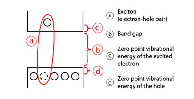
As the confinement energy depends on the quantum dot's size, both absorption onset and fluorescence emission can be tuned by changing the size of the quantum dot during its synthesis. The lifetime of fluorescence is determined by the size of the quantum dot. Larger dots have more closely spaced energy levels in which the electron-hole pair can be trapped. Therefore, electron-hole pairs in larger dots live longer causing larger dots to show a longer lifetime.
2.3 Applications of Quantum Dots
Tuning the size of quantum dots is attractive for many potential applications. For instance, larger quantum dots have a greater spectrum-shift towards red compared to smaller dots, and exhibit less pronounced quantum properties. Conversely, the smaller particles allow one to take advantage of more subtle quantum effects.
Biological applications
The use of quantum dots for highly sensitive cellular imaging has seen major advances. The improved photostability of quantum dots, for example, allows the acquisition of many consecutive focal-plane images that can be reconstructed into a high-resolution three-dimensional image. Another application that takes advantage of the extraordinary photostability of quantum dot probes is the real-time tracking of molecules and cells over extended periods of time. Antibodies, streptavidin, peptides, DNA, nucleic acid aptamers, or small-molecule ligands can be used to target quantum dots to specific proteins on cells.
Optical applications
So far, quantum dots have attracted most interest because of their interesting optical properties: they're being used for applications where precise control of coloured light is important.
Quantum dots are also being hailed as a breakthrough technology in the development of more efficient solar cells. In a traditional solar cell, photons of sunlight knock electrons out of a semiconductor into a circuit, making useful electric power, but the efficiency of the process is quite low. Quantum dots produce more electrons (or holes) for each photon that strikes them, potentially offering a boost in efficiency of perhaps 10 percent over conventional semiconductors. CCDs (charge-coupled devices) and CMOS sensors, which are the image-detecting chips in such things as digital cameras and webcams, work in a similar way to solar cells, by converting incoming light into patterns of electrical signals; efficient quantum dots could be used to make smaller and more efficient image sensors.
Quantum dots are also finding their way into computer screens and displays
In a typical LCD (liquid crystal display screen), combinations of red green and blue crystals (effectively colour filters, which are turned on or off depending on tis need) that are illuminated from behind by a very bright backlight.
Quantum Dots offer a few advantages over LCD screens.
First, Quantum dots naturally produce monochromatic light, they can be more efficient than light sources which must be colour filtered.
Second, if Quantum Dots are applied as a way of eliminating the need for White LED backlights and colour filters, they reducing power consumption, and increase the accuracy of contrast.

Third, quantum dots are much smaller than liquid crystals so they'd give a much higher-resolution image.
Quantum Dot Light Emitting Diodes can be fabricated on a silicon substrate, which allows them to be integrated onto standard silicon-based integrated circuits or microelectromechanical systems.
Quantum Computing
As computers get faster and smaller, a time will come when the physical limits of materials prevent them advancing any further—unless we develop entirely different technologies. One possibility would be to store and transmit information with light instead of electrons—a technology broadly known as photonics. Optical computers could use quantum dots in much the same way that electronic computers use transistors (electronic switching devices)—as the basic components in memory chips and logic gates.
Conclusion
Nanoparticles today are still a field of high research output; for example, in January 2019, researches at Indian Institute of Technology (IIT) Madras found that unlike bulk silver, silver nanoparticles are not rigid and fixed at specific locations as we thought them to be. Such dynamics can occur in any nanosystem. Fundamental insight the study provides is that nanoparticles are indeed molecules.
Nanoparticles have been used for a long time. The medieval artisans were unaware that they were using nanotechnology. They just knew that a particular process produced a beautiful effect. Now, we have looked deeper into the properties and structures of these nanoparticles and have constructive evidence to claim that the particles’ properties depend directly on their shape and structure. By manipulating these factors, we can create nanoparticles specialised to our uses. The use of nanoparticles has now extended to fields like quantum computing, solar cells, and display panels.
As we move towards a future where everything will become smaller, nanoparticles are a boon to mankind.
Bibliography
1. Satoshi Horikoshi and Nick Serpone [2013] Introduction to Nanoparticles
2. Rao, CNR; Thomas, PJ; Kulkarni, G.U [2007] Nanocrystals : Synthesis, properties and Applications
3. Wood, R.W. (1902) Proc. Phys. Soc. London ; Wood , R.W. (1902) Philos. Mag ; Wood, R.W. (1912) Philys. Mag.
4. Rayleigh, L (1907) Proc. R. Soc. London Ser. A
5. Otto, A.(1968) Z. Phys.
6. Kretschmann, E. , and Raether, H. (1968) Z. Naturforsch.
7. Van Driel; A. F. (2005). Frequency-Dependent Spontaneous Emission Rate from CdSe and CdTe Nanocrystals: Influence of Dark States
8. Yu, M.-F.; Lourie, O; Dyer, MJ; Moloni, K; Kelly, TF; Ruoff, RS (2000). Strength and Breaking Mechanism of Multiwalled Carbon Nanotubes Under Tensile Load
9. Reibold, M.; Paufler, P; Levin, AA; Kochmann, W; Pätzke, N; Meyer, DC (16 November 2006). Materials: Carbon nanotubes in an ancient Damascus sabre
10. Sanderson, K. (2006). Sharpest cut from nanotube sword
11. Liu, F.; Wagterveld, R.M., Gebben, B., Otto, M.J., Biesheuvel, P.M., Hamelers, H.V.M. (2014). Carbon nanotube yarns as strong flexible conductive capacitive electrodes
12. Jin, R; Cao, Y; Mirkin, C.A; Kelly, K.L; Schatz, G.C and Zheng, J.G. (2001) Science Iss 294
13. Schasfoort, R.B.M. and Tudos, A.J (2008) Handbook of Surface Plasmon Resonance
14. Sugimoto, T (2000) Fine Particles: Synthesis, Characterization, and Mechanisms of Growth, Surfactant Sci. Series Vol. 92
15. Kreibig, U. and Vollmer, M. (1995) Optical Properties of Metal Clusters
16. Радушкевич, Л. В. (1952). О Структуре Углерода, Образующегося При Термическом Разложении Окиси Углерода На Железном Контакте
17. Wang, X.; Li, Qunqing; Xie, Jing; Jin, Zhong; Wang, Jinyong; Li, Yan; Jiang, Kaili; Fan, Shoushan (2009). Fabrication of Ultralong and Electrically Uniform Single-Walled Carbon Nanotubes on Clean Substrates
18. Zhou, Junshuang; Li, Na; Gao, Faming; Zhao, Yufeng; Hou, Li; Xu, Ziming (2014). Vertically-aligned BCN Nanotube Arrays with Superior Performance in Electrochemical capacitors". Scientific Reports
http://www.trustedreviews.com/opinion/quantum-dots-explained-what-they-are-and-why-they-re-awesome-2916068
http://www.explainthatstuff.com/quantum-dots.html
http://www.britishmuseum.org/explore